


Single metal thermocouples (SMTs) have recently been developed with a new design concept of width-engineering of metal segments. In such designs, two segments of different micro-width are formed to obtain different levels of Seebeck effects. The variations in the Seebeck effect achieved from dissimilar segment width are small. In addition, the fabrication of such micro-width patterns requires special fabrication facilities such as photolithography or electron-beam lithography. In this article, an alternative method is presented that has the potential to give high thermal sensing SMTs and requires no sophisticated facilities to fabricate. The method is based on thickness-engineering instead of width-engineering, and thus devices can be obtained from commonly available thin film deposition techniques. Constructing better thermal sensing SMTs is possible with this approach as thickness can be easily and conveniently varied down to nanoscale range, which is necessary to achieve significant changes in the Seebeck effects from effectively using size effects. As a result, a high thermal sensing bismuth based-SMT has been fabricated with a sensitivity of as high as 31μVK-1, one of the highest values reported for SMTs. It is straightforward, more convenient over width-engineering approach and thus SMTs can be easily developed.
1 Introduction
Thermocouples, a universal type of thermometer, are typically made up of two dissimilar metals [1, 2]. These devices work on the principle of the Seebeck effect and, therefore, the use of two metals of dissimilar Seebeck coefficients is a basic requirement to observe a voltage signal from these sensors [1]. When two dissimilar metals/conductors of different Seebeck coefficients (S1 and S2) are joined to form a thermocouple junction, an open circuit voltage signal can be observed by heating or cooling the junction. The magnitude of this voltage (∆V) is directly proportional to (i) temperature difference (∆T) between the junction and open ends of the metals and (ii) difference between the Seebeck coefficients (S1 and S2) of metals, which can be expressed as [1]:
![]() where S1 and S2 are the Seebeck coefficients of metal 1 and 2, respectively.
where S1 and S2 are the Seebeck coefficients of metal 1 and 2, respectively.
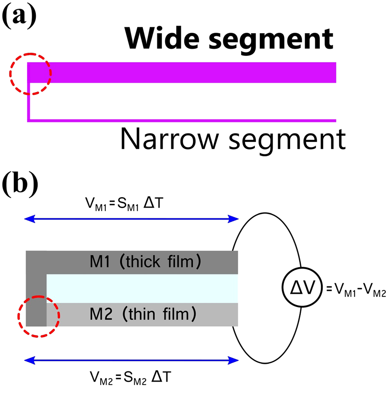
Alternatively, researchers have come up with a new concept of “single metal thermocouple” (SMT) in which a single metal layer with two segment patterns of different widths are used, as illustrated in Figure 1a [1–4]. In these width-engineered patterns with at least one of the segments of narrow width, the Seebeck coefficient can be modified with respect to the wider segment to obtain a net voltage from the sensor. As they need micrometer wide patterns, the construction of the width-engineered thermocouples requires special fabrication techniques such as photolithography or electron-beam lithography [1, 2, 5, 6]. Further, due to the limitations of reducing the width down to the sub-100nm range, the thermoelectric changes between the wide and narrow segment are also limited. As a result, most of the reported width-engineered SMTs have low thermal sensitivity of about 1-5μVK-1. Here, an alternative and straightforward method to fabricate SMTs has been developed that overcomes the above difficulties, enabling the construction of SMTs with better thermal sensitivity. The method is based on thickness variation of the metal patterns instead of width, as the thickness of the patterns can be easily and conveniently varied or controlled in the nanoscale range with common thin film deposition techniques (Figure 1b). As a proof of concept, a bismuth-based thickness-engineered SMT has been designed and developed that shows a high thermal sensitivity of 31μVK-1, one of the highest values reported in SMTs.
2 Experimental details
2.1 Thin film fabrication
For initial thermoelectric testing, bismuth (Bi) thin films of different thickness (t ∼ 500nm, 200nm, 100nm, 50nm, 20nm) on glass substrates have been deposited by the sputter coating method (Model: Quorum Q150T S coater) using a bismuth target (99.9% purity, PI-KEM Ltd). For every deposition run, the sputtering chamber was evacuated to 10-4 mbar and films were deposited at room temperature under an argon atmosphere (10-2 mbar). A sputter current of 20mA was used for all the films and thickness was controlled using the film thickness monitor accessory of the instrument.
2.2 Fabrication of single metal thermocouple (SMT)
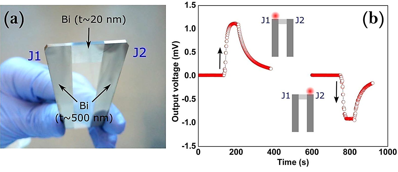
The SMT device consisting of two Bi layer strips/segments of t ∼ 20nm and 500nm was patterned on a microscope glass slide (size: 75mmÅ∼25mm). To fabricate this device as illustrated in Figure 1b, first, a thin metal layer strip (t ∼ 20 nm, width: 8mm) was deposited and then an L-shaped thick metal layer (t ∼ 500 nm, width: 8mm) using a mask. Another SMT device having two junctions was fabricated by patterning a thin metal layer (t ∼ 20 nm) between the two thick metal layers (t ∼ 500 nm).
2.3 Measurements and characterization
The Seebeck coefficient measurements on Bi thin films of different thickness were performed using a standard method with a homemade setup [7]. The thermoelectric voltage (∆V) produced from the thin film samples have been recorded at different temperature gradients (∆T), and the Seebeck coefficients were estimated using the expression, S = —(∆V/∆T) [8, 9]. The electrical resistivity of the films was obtained from the standard four-probe method. The output characteristics of the SMT sensors were performed by heating the junction to different temperatures and recording the output voltage signal. The junction heating was achieved from a small resistive heater (size: 5mmÅ∼5 mm, thickness: 1 mm, resistance: 100Ω) [10] by supplying DC-power inputs. This heater and a K-type thermocouple were fixed on a thin copper plate (thickness ∼ 0.5mm) of similar size as the heater using high-temperature glue; the resulting heating element was then placed on the junction area of the SMT. Good physical contact between the heating element and junction was maintained by a pressing arrangement with a spring clamp set. All the thermoelectric voltages of the individual films and the output voltage signal of SMT sensors were measured with micro-voltmeters (Model:HMC8012DMM). The DC-voltage accuracy for this model of multimeter is 0.015% of reading +0.002% of range. So, for the most precise range of 400.000 mV, the best accuracy would be about 8 μV. The surface morphology of the junction area of a sensor was obtained by scanning electron microscopy (SEM) using a Zeiss Evo LS25 SEM.
3 Results and discussion
The proposed thickness-engineered design of a single metal thermocouple (SMT) based on different thickness metal layers is schematically displayed in Figure 1b. Bi metal has been chosen for the purpose due to its more prominent thermoelectric changes with respect to the changes in the material dimension, and, also, it is one of the metals to display substantial thermoelectric effects, as compared to any other metal [11, 12]. The changes in the thermoelectric effects have been confirmed by measuring the Seebeck coefficient (S) of the individual Bi films of different thickness; the data is shown in Figure 2a. The observed room temperature S value of a 500nm thick film is —52μVK-1, which has seen a decreasing trend with respect to reduction of film thickness; —46μVK-1, —39μVK-1, —21μVK-1, and —15μVK-1 are the S values of the films having thickness 200 m, 100nm, 50nm, and 20nm, respectively. The reduction in the Seebeck coefficient in thin films as compared to their bulk values has been observed in most of the metal films due to the increased electron scattering at the surface and theoretically described by the Fuchs-Sondheimer model [1, 13, 14]. The variation of resistivity as a function of film thickness is shown in Figure S1 (available online at stacks.iop.org/ERX/3/035015/mmedia) (supplementary file); the resistivity of the thick film (t ∼ 500 nm) is found to be 5.4Å∼10-4Ωcm, which is slightly more than its bulk resistivity and consistent with previously reported values for Bi thin film [12, 15]. With the decrease in film thickness, it is found to increase as shown in Figure S1 (supplementary file). This increase is attributed to the fact that charge carriers in thin films undergo scattering at the film surface, which is more pronounced in the case of very thin films.
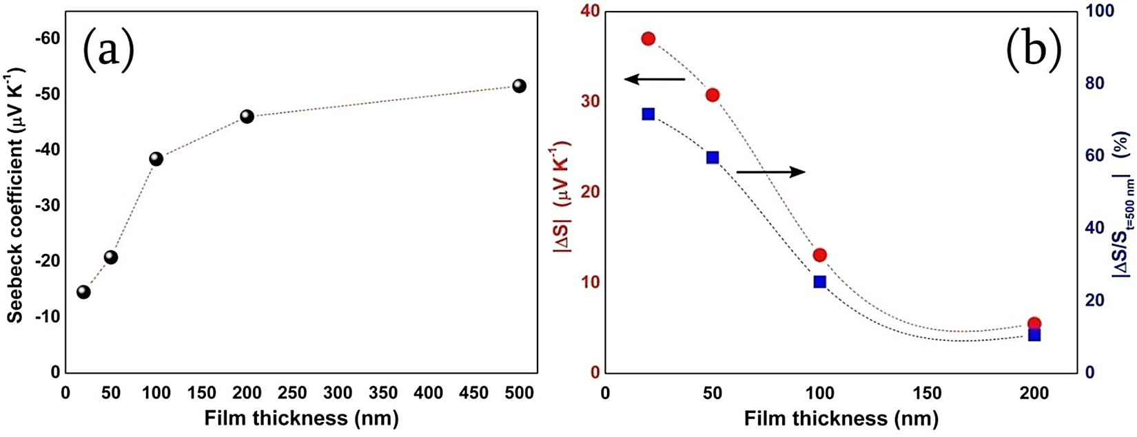
|ΔS/St=500nm|, on the films of thickness, t ~ 200nm, 100nm, 50nm, and 20nm with respect to the first film of t ~ 500nm.
The dependence of absolute values of S reduction, |∆S|, on the films of thickness, t ∼ 200nm, 100nm, 50nm, and 20nm with respect to the first film (t ∼ 500nm) are shown in Figure 2b with an observed maximum |∆S| for the film with t ∼ 20nm. The change of S from —52μVK-1 to —15μVK-1 demonstrates a very high relative reduction of Seebeck coefficient |∆S/St=500 nm| of about 70%, which is higher than values achieved in width-controlled segments. For illustration, a maximum relative reduction of Seebeck coefficients of about 30% to 35% was reported in Ta and Ti metals by decreasing the segment width from 100μm to 3μm[14] . But in the case of Bi, the reduction of segment width to 3μm has resulted in a less than 6% reduction [14] . These data indicate that the thickness-engineered sensors can have better output signal or thermal sensitivity in contrast to the width-engineered sensors. The changes in the Seebeck coefficient with respect to material dimension can be understood through standard expressions, such as the Mott-Jones equation for S (in metals), which is expressed as [14 , 16]
 where kB, σ, e, T, E, and Ef are Boltzmann constant, electrical conductivity, the charge of the electron, temperature, electron energy, and the Fermi energy, respectively. As the electrical conductivity (σ) in metals can be expressed by [14]
 where λ, A, and h are the mean free path of charges, Fermi surface area, and the Plank’s constant, respectively, the equation for S can be divided into two parts [14]:
 The variations to the S from the second term in the above equation are not expected as the term (dlnA/dE)E=Ef can change in the case of atomic-scale material dimensions, hence the second term is approximately considered constant [14]. Therefore, the size effects on the S are in general dominated by the first term (related to λ) . It is well-known that surface scattering is an additional mechanism that occurs in thin films in addition to the phonon, impurity, and defect-scattering mechanisms [13]. The surface scattering can influence the S and other transport properties when the thickness is comparable to the mean free path (λ) of the charge carriers (for most metals, the range of λ is about 40-100nm) [13, 14]. Therefore, the bulk S values can be changed by reducing at least one of the dimensions to nanoscale and significant changes in S can be expected in thin films of nanoscale thickness as compared to microscale width-engineered patterns.
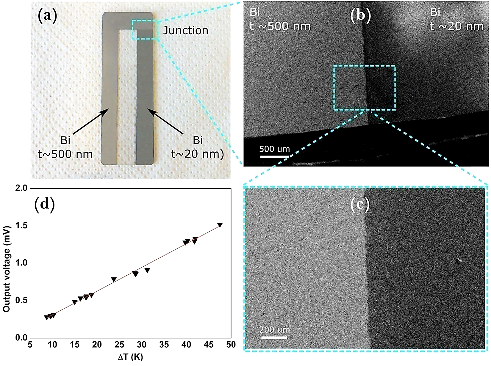
The photograph of SMT displayed in Figure 3 has two segments of t = 500nm and 20nm as the maximum difference in the Seebeck coefficient |∆S| can be obtained from this combination. The surface morphology of the films and the junction region are also given in Figure 3, which show the morphological differences between the thick and thin film. The open-circuit voltage (∆V) as a function of temperature gradient (∆T) is shown in Figure 3d; a linear increase in the ∆V with respect to the increase in ∆T has been observed with a slope value of 31μVK-1, one of the highest sensitivity values from the SMTs reported until now. The observed sensitivity is in near agreement with the estimated ∆S = 37μVK-1 from S values of the individual segments of t = 500nm and 20nm. The output signal data points are well aligned with linear fittings with a good R2 value of 0.995, which suggests that the sensor has a nearly constant sensitivity factor and can be useful for thermal sensing applications around room temperature. These measurements were carried out at a room temperature of ∼21± 2°C and the devices can be used up to ∼80°C without any problems. The small decrease in the observed sensitivity of the thermocouple as compared to the estimated ∆S might be associated with the uncertainties in the junction heating temperatures. Previous work on a Pd thin film SMT with dual strips of widths 30µm–200nm has reported a maximum sensitivity of 2.2μVK-1 and for a Ni film based SMT with strips widths 100μm-3μm, a maximum sensitivity of 1.1μVK-1 has been reported [2 , 5]. Recent studies suggest that the high thermal sensitivity values as compared to metal-based devices can be observed in carbon or graphene-based devices [4 , 17].
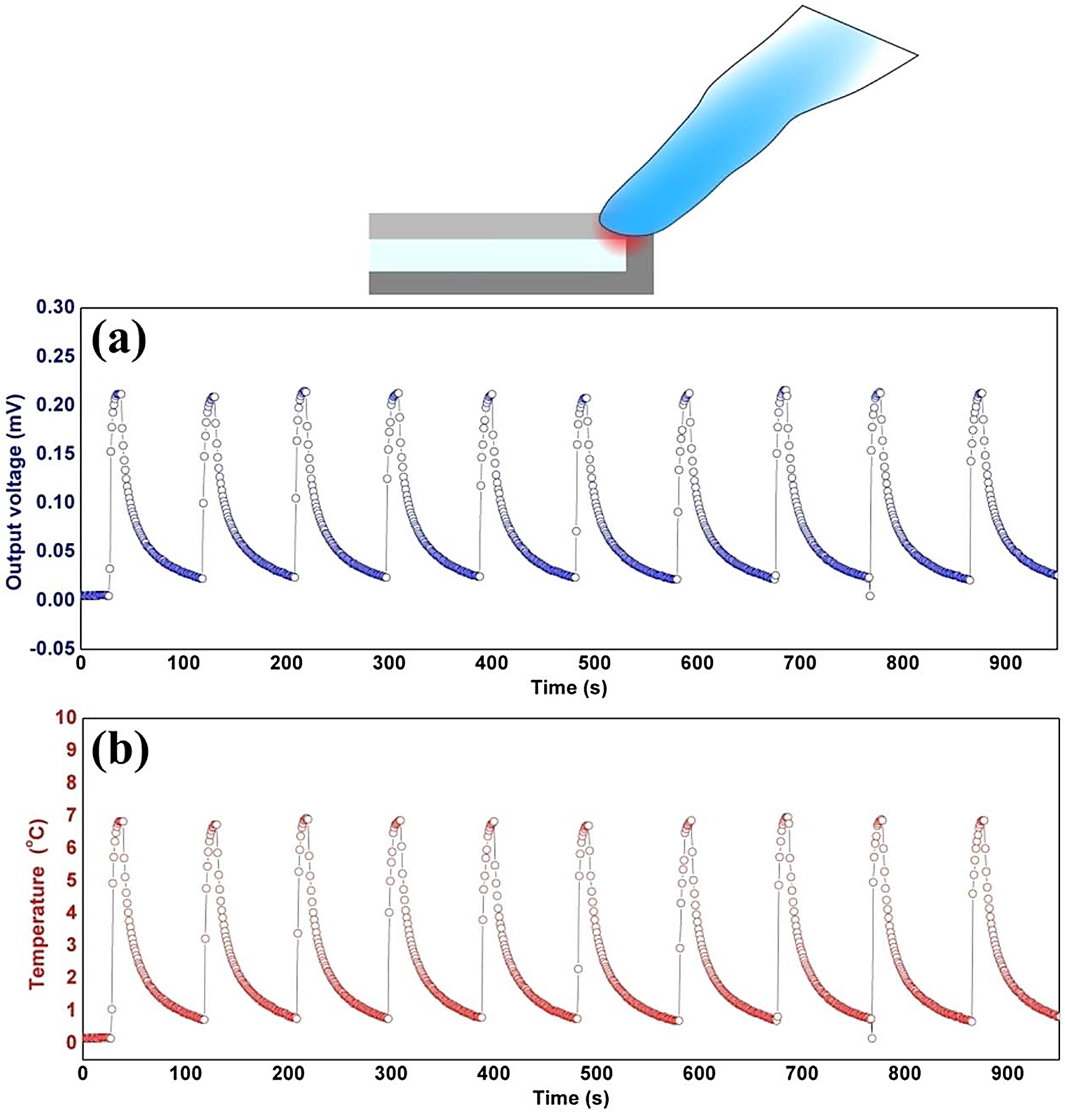
The sensing capability and reliability of the Bi SMT have been studied under a continuous and cyclic operation by touching the junction with a finger wearing a nitrile glove for 10 seconds and recording the generated signal from the SMT. As shown by Figure 4a, a sharp increase in the voltage signal is observed for each touching cycle and the observed maximum voltage is consistent. The observed voltage signal is then converted into temperature by using the thermal sensitivity value of 31μVK-1 in order to realize the temperature change before and after touching the sensor; the data of which is plotted in Figure 4b. The observed peak values from the 10 repetitive touching cycles are found to be in the range of 6.70°C to 6.96°C with an estimated average value of 6.85(±0.08)°C (the data scatter rang e±0.08°C was estimated from 10 peak temperature values of the heating cycles). Further, the reliability of this observed temperature change from the Bi SMT was confirmed by a similar procedure with a standard K-type thermocouple sensor; the rise in temperature was recorded by touching it with a gloved finger for a similar time period of 10 seconds. The recorded variation in the temperature is shown in Figure S2 (supplementary file); the temperature reading has changed from 21.3°C (room temperature) to 27.8°C before removing the finger after 10 seconds, which indicates a net change of 6.5°C. These measurements confirm that the SMT is giving reliable information, the small difference between the temperature data from the SMT and standard K-type thermocouple, which is about 0.3°C, could be due to the variations in the pressure applied by the finger or the pressing time. Further, the thermal response time of the SMT is very short, which is evident from the sharp rise of the voltage signal observed immediately after touching the sensor; a magnified single curve has been shown in Figure S3 (supplementary file).
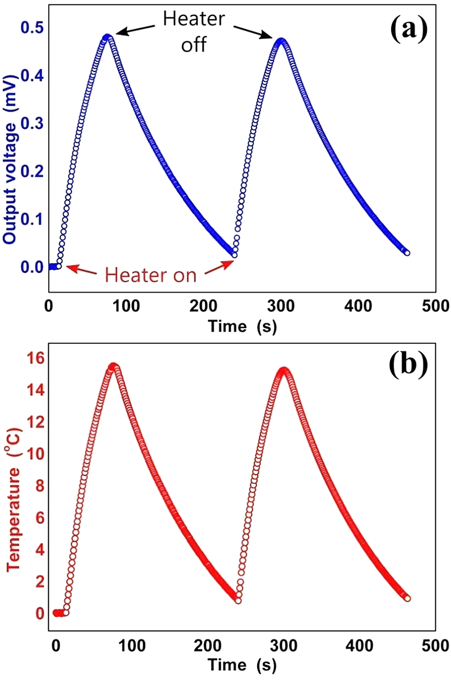
The sensing reliability of the SMT under heating cycles was also studied by heating with a standard resistive heater fixed on the junction; Figure 5 shows data of two heating cycles. The heater was applied with a fixed DC power for ∼1 minute and turned off, the output voltage variation of the SMT was recorded; a similar procedure was repeated to record sensing data for the second heating cycle. The sensor output voltage was then converted into temperature using its thermal sensitivity value (see Figure 5b). The temperature change of ∼15.5°C was observed from the SMT sensor whereas the temperature of the standard thermocouple attached to the heater changed from 21.7°C to 37.6°C resulting in a net change of 15.9°C. These results indicate that the present SMT sensors can produce reliable thermal sensing data.
The dissimilar Seebeck effects in Bi film segments of different thickness have also been observed and confirmed with a design of a two-junction (J1 and J2) pattern. For this, a thin film segment (t ∼ 20nm) was deposited between two thick film segments (t ∼ 500nm) as shown in Figure 6. When one of the junctions was heated using a small resistive heater placed on one of the junctions, there was a voltage generation from the pattern and also, there was a change in the polarity of the output voltage when the hot junction was changed from J1 to J2 or vice-versa; the output voltage response is presented in Figure 6b. This confirms that the change in the direction of net flow of charges through the pattern made up of Bi films of different thickness due to different levels of Seebeck effects in the segments. Overall, the present study demonstrates that the changes in thermoelectric powers of Bi metal are small in microscale and thus significant changes can be observed by going down to nanoscale, which can be easily and effectively achieved by varying thickness instead of the width of the segments.
In addition, studies on Bi thin films and nanowires have reported a significantly decreased thermal conductivity in contrast to its bulk value [18–21]. Good Seebeck coefficient and good electrical conductivity added with reduced thermal conductivity can make this element a promising n-type material [22 , 23] and can be used in combination with good p-type thermoelectric materials for low temperature heat conversion applications [24–29].
4 Conclusions
The present work introduces an alternative method to achieve higher thermal sensitivity from the single metal thermocouples (SMT). More prominent changes in the Seebeck coefficient can be observed by changing the metal film thickness instead of width and, as a proof of concept, high thermal sensitivity of 31μVK-1 has been achieved in thickness-engineered Bi-based SMT constructed from a combination of 500nm and 20nm thick segments. The fabrication of thickness-engineered SMTs is simple and does not require any special facilities, which makes the approach more preferable and economical.
Acknowledgments
Authors are thankful to the Welsh Government (EUEuropean Regional Development Fund) for funding the RICE (Reducing Industrial Carbon Emission) project (Grant Number: 81435). Authors would like to acknowledge the assistance provided by Swansea University College of Engineering AIM Facility, which was funded in part by the EPSRC (EP/M028267/1), the European Regional Development Fund through the Welsh Government (80708), and the Ser Solar project via Welsh Government.
Data availability statement
All data that support the findings of this study are included within the article (and any supplementary files).
Conflicts of interest
The authors declare that they have no conflict of interest.
References
- Szakmany GP, OrlovAO, Bernstein GH, and Porod W; 2014 Single-metal nanoscale thermocouples IEEE Trans. Nanotechnol. 13 1234–9
- Liu H, Sun W,and Xu S; 2012 An extremely simple thermocouple made of a single layer of metal Adv. Mater. 24 3275–9
- Huo X, Xu J, Wang Z, Yang F, and Xu S; 2016 Performance of nano-submicron-stripe Pd thin-film temperature sensors Nanoscale Res. Lett. 11 351
- Harzheim A, Könemann F, Gotsmann B, van der Zant Hand Gehring P; 2020 Single-material graphene thermocouples Adv. Funct. Mater. 30 2000574
- Huo X, Liu H, Liang Y, Fu M, Sun W, Chen Q,and Xu S; 2014 A nano-stripe based sensor for temperature measurement at the submicrometer and nano scales Small 10 3869–75
- Balčytis A, Ryu M, Juodkazis S, and Morikawa J; 2018 Micro-thermocouple on nano-membrane: thermometer for nanoscale measurements Sci. Rep. 8 6324
- Mulla R and Rabinal MK; 2016 A simple and portable setup for thermopower measurements ACS Combinatorial Science 18 177–81
- Mulla R, Glover K, and Dunnill CW; 2021 An easily constructed and inexpensive tool to evaluate the Seebeck coefficient IEEE Trans. Instrum. Meas. 70 1–7
- Wang C, Chen F, Sun K, Chen R, Li M, Zhou X, Sun Y, Chen D, and Wang G; 2018 Contributed review: instruments for measuring Seebeck coefficient of thin film thermoelectric materials: a mini-review Rev. Sci. Instrum. 89 101501
- Mulla R and Rabinal MK; 2019 A tweezer as a thermoelectric tester Phys. Educ. 54 055032
- Mikolajczak P, Piasek W, and Subotowicz M; 1974 Thermoelectric power in bismuth thin films Phys. Status Solidi (A) 25 619–28
- Rogacheva EI, Grigorov SN, Nashchekina ON, Lyubchenko S, and Dresselhaus MS; 2003 Quantum-size effects in n-type bismuth thin films Appl. Phys. Lett. 82 2628–30
- Das VD and Soundararajan N; 1987 Size and temperature effects on the Seebeck coefficient of thin bismuth films Phys. Rev. B 35 5990–6
- Sun W, Liu H, Gong W, Peng L-M, and Xu S-Y; 2011 Unexpected size effect in the thermopower of thin-film stripes J. Appl. Phys. 110 083709
- Kumar A and Katyal OP; 1990 Electrical resistivity of thin bismuth films J. Mater. Sci., Mater. Electron. 1 51–6
- Mulla R and Rabinal MHK; 2019 Copper sulfides: earth-abundant and low-cost thermoelectric materials Energy Technology 7 1800850
- Mulla R, Jones DR, and Dunnill CW; 2020 Thermoelectric paper: graphite pencil traces on paper to fabricate a thermoelectric generator Adv. Mater. Technol. 5 2000227
- Song DW, Shen WN, Dunn B, Moore CD, Goorsky MS, Radetic T, Gronsky R ,and Chen G; 2004 Thermal conductivity of nanoporous bismuth thin films Appl. Phys. Lett. 84 1883–5
- Kim G-S, Lee M-R, Lee S-Y, Hyung J-H, Park N-W, Lee E S. and Lee S-K; 2013 Reduction in thermal conductivity of Bi thin films with high-density ordered nanoscopic pores Nanoscale Res. Lett. 8 371
- Lee S-Y, Kim G-S, Lee M-R, Lim H, Kim W-D,and Lee S-K; 2013 Thermal conductivity measurements of single-crystalline bismuth nanowires by the four-point-probe 3-ω technique at low temperatures Nanotechnology 24 185401
- Holtzman A, Shapira E, and Selzer Y; 2012 Bismuth nanowires with very low lattice thermal conductivity as revealed by the 3ω method Nanotechnology 23 495711
- Goldsmid HJ; 2006 Bismuth—the thermoelectric material of the future? 2006 25th International Conference on Thermoelectrics pp 5–10
- Mulla R and Dunnill CW; 2021 Fabrication of wooden thermoelectric legs to construct a generator Green Materials 1–6
- Mulla R, Jones DR, and Dunnill CW; 2020 Economical and facile route to produce gram-scale and phase-selective copper sulfides for thermoelectric applications ACS Sustainable Chemistry&Engineering 8 14234–42
- Mulla R and Dunnill CW; 2019 Powering the hydrogen economy from waste heat: a review of heat-to-hydrogen concepts ChemSusChem 12 3882–95
- He Y, Day T, Zhang T, Liu H, Shi X, Chen L, and Snyder GJ; 2014 High thermoelectric performance in non-toxic earth-abundant copper sulfide Adv. Mater. 26 3974–8
- Chen X, et al; 2019 Carbon-encapsulated copper sulfide leading to enhanced thermoelectric properties ACS Appl. Mater. Interfaces 11 22457–63
- Mulla R and Dunnill CW; 2020 Graphite-loaded cotton wool: a green route to highly-porous and solid graphite pellets for thermoelectric devices Composites Communications 20 100345
- Liu W-D, Yang L, Chen Z-G, and Zou J; 2020 Promising and eco-friendly Cu2X-based thermoelectric materials: progress and applications Adv. Mater. 32 1905703
About the authors
Rafiq Mulla and Charles W. Dunnill are with the Energy Safety Research Institute, Swansea University, Bay Campus, Fabian Way, Swansea SA1 8EN, United Kingdom. © 2021 The Author(s).
Published by IOP Publishing Ltd (https://iopscience.iop.org/article/10.1088/2631-8695/ac144f)
This is an open access article under the terms of the Creative Commons Attribution 4.0 license (https://creativecommons.org/licenses/by/4.0). It has been edited to conform to the style of Thermal Processing magazine.


 general practice for CQI-9 and AMS2750E")


