


Thin-film thermocouple (TFTC) technology is a novel measurement method that produces a thermocouple sensor during the deposition process, even though it is a complex surface, to obtain the surface temperature. TFTC is a thin film sensor for measuring temperature by contact methods, consisting of two different metals that can generate thermoelectric forces named “Seebeck effects.” In the past decade, there have been many attempts to measure the cutting temperature during machining processes using TFTF sensors. However, research has not yet progressed to optimize the sensor performance or fabrication process. This article studies a preliminary technique for the fabrication of a TFTC sensor on a cutting tool surface and optimizes the deposition conditions, TFTC design, and sensor performance. Chromel and Alumel, which are materials commonly used in K-type thermocouples, were used for the thermal evaporation process. When the Chromel has a nickel-to-chrome ratio of 9:1, low resistivity and minimal variation with increasing temperature were observed. When the contact area of the deposited electrode (+) and (−) poles increased, the resistivity decreased, and the TFTC sensitivity improved. Data acquisition tests using a DAQ system connected to the TFTC sensor show the lowest resistivity in TFTC B and C types are able to measure temperature data. It is expected that the heat generated during the cutting process can be detected using the TFTC sensor with B-type shape and Chromel with a 9:1 nickel-to-chrome ratio.
1 Introduction
The cutting temperature is a key factor in determining product quality and operation efficiency for machining processes. When a tool contacts the workpiece for the depth of the cut, the result is high-heat generation on the tool, chip, and workpiece. The generated heat energy reaches a temperature of about 1,200°C, depending on the processing conditions. The heat sources are in the frictional, shear, and flank zones at the tool-chip interfaces. The frictional zone has the highest cutting temperature among the heat sources. Frictional heat leads to crater wear, which causes failure, such as tool fracture, shortened tool life, and low-surface integrity. For the reasons presented above, manufacturer and engineer efforts have been made to control cutting temperature generated during the machining process. Up to recently, the cutting temperature has been investigated through experimental measurements and simulation techniques.
Numerical simulation techniques are valuable for predicting cutting temperatures. Tool wear rate can be calculated by the wear model proposed by Usui et al. [1], which is dependent on the contact stress and cutting temperature. Tiffe et al. [2] found optimal cutter edge profiles to reduce tool temperature using the finite element method (FEM) technique. The edge profiles had complex shapes, and the results of their work were beneficial for analyzing the thermal gradient and how it affects tool life. Childs et al. [3] investigated the relationships between temperature, force, and chip geometry for a wide range machining conditions of Ti-alloys using the FEM technique. Elevated temperature influenced the shear failure of Ti64 and the critical strain. The simulated predicted temperature is valuable data for analyzing the cutting mechanisms with changing material properties and failures. Some industries have strict regulations on surface quality; therefore, cutting result predictions are important. Machining temperature is often the main factor that changes material properties, such as microstructure. Imbrogno et al. [4] predicted microstructural and microhardness depending on machining temperature and its effect on surface integrity. As seen in the literature discussed above, machining simulations are useful for assessing the metal-cutting process by predicting cutting temperatures. However, validation is necessary to ascertain the simulation and temperature measurement during machining is required to compare simulated and experimental results.
Many researchers have developed cutting temperature measurement techniques for use during machining operations. These measurement techniques are categorized as contact and non-contact methods. The contact method is applicable in single-point metal cutting processes, such as the turning process. A turning tool does not rotate, unlike tools used in the multi-point metal cutting process. Installing thermocouples onto the cutter is the most typical and easy method for measuring the cutting temperature. Bagherzadeh et al. [5] measured cutting temperature during the cryogenic turning process. The drilled hole of the insert using electrical discharge machining (EDM) is close to the cutting edge. Although using a thermocouple is a stable assessment method, it indirectly measures heat generation from tool-chip interfaces that is transferred through the insert body. Thermal imaging is also a good non-contact technique for determining temperature distributions at tool-chip interfaces. An infrared (IR) camera detects temperature through infrared radiation (IR) during thermal imaging, which has gained significant attention in the machining processes. The IR imagining technique has a constraint of measuring temperature due to cutting fluids [6]. Another non-contact measurement technique involves the use of a two-color fiber pyrometer. This method is analogous to a thermocouple and identifies the data within the spot size (∼500 µm). The pyrometer is based on material radiation detection and a predefine term for the emissivity is required [7]. Thermosensitive paints have shown relative variances of temperature but have no way to determine the amount of variation [6]. As indicated in published work, conventional thermal measurement techniques have limitations in obtaining accurate tool-chip interface temperature.
The thin-film thermocouple (TFTC) is a novel technology developed in recent decades and functions as a thermocouple sensor on flat, curved, or any type of surface. Even their small thermal mass allows for significantly faster response times compared to conventional wire sensors [8,9]. Basti et al. [10] deposited TFTCs of Ni-(Ni-Cr) on an alumina cutting tool and fabricated junctions to measure cutting temperatures. TFTC sensor data is suitable for measuring temperature and exhibits a corresponding trend in cutting force variance [10,11]. Werschmoeller et al. [[12], [13], [14]] attempted fabrication of a micro-arrayed TFTC sensor on a polycrystalline cubic boron nitride (PCBN) cutting tool. The advantage of a micro-arrayed TFTC is the measurement of temperature maps by interpolation. A three-dimensional (3D) map of the data is available instead of thermal imaging data. Li et al. [15] embedded micro-TFTC sensor arrays on a PCBN cutter surface and recorded cutting temperatures. The micro-TFTC has an array design to measure multiple points in the temperature field. TFTC sensors can be used to detect progressive wear. The flank face of the tool is significant to the surface quality. Li et al. [16] and He [17] devised TFTC development process on the flank face of a tool for real-time monitoring of wear progression. The TFTC on the flank face was manufactured in a similar process as that in [15]. The previously mentioned literature indicates the typical TFTC fabrication method is deposition by a sputtering method. The deposited material adheres to the surface. However, high pressures due to the cutting forces damage TFTC sensors.
The strategy for protecting TFTC sensors from extreme friction and temperature is a great challenge because of the damage imparted to the thin-filmed sensor during cutting processes. Kesriklioglu et al. [18] embedded a K-type thermocouple TFTC. In their study, an AlTiN layer coated the upper side on layers of Chromel and Alumel to protect the TFTC sensor. Li et al. [19] suggested a micro-textured tool with a deposited TFTC sensor. The texture of their proposed tool has a depth of about 100 µm via laser beam, while Alumel and Chromel were coated inside the texture using plasma-enhanced chemical vapor deposition (PECVD). Molybdenum disulfide filled in the grooves and acted as a lubricant at the tool-chip interfaces to protect the fabricated TFTC sensors. The micro-textured TFTC sensor exhibited significantly improved performance during the machining process. This design improved the protection of the TFTC sensors under high-pressure and high-temperature environments. However, the preparation process for the fabrication of the grooved tool was inadequate because the complicated procedure was high in cost and time consuming [19, 20, 21].
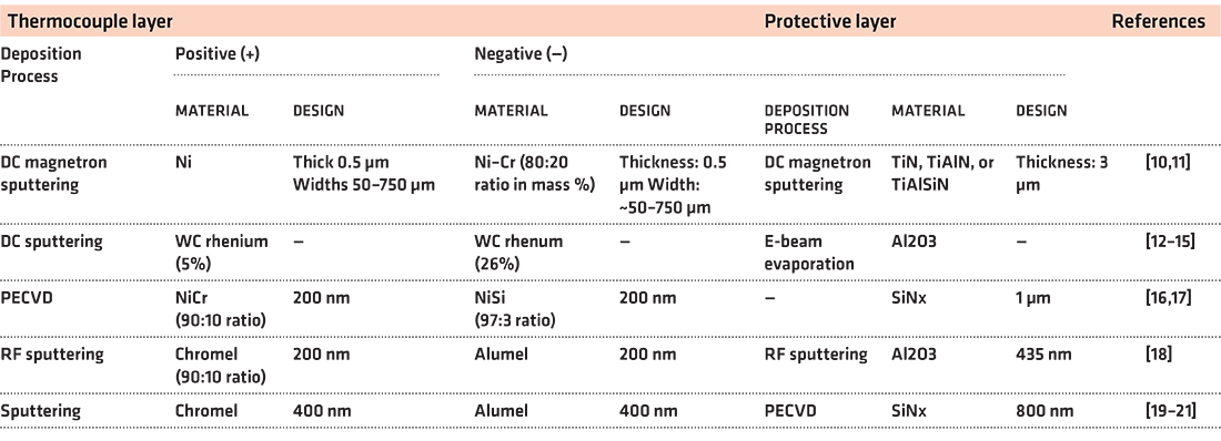
Table 1 provides a summary of published papers describing TFTC techniques. In the literature, the material combination used for TFTC fabrication was equal to compositions of C- or K-type thermocouples generating electromotive force. The most-used deposition method for the TFTC layer was sputtering. The coating methods used to create the protective layer varied and included methods such as sputtering, e-beam evaporation, and PECVD. Only a few studies have investigated the TFTC fabrication process and design parameter studies for circuit dimensions have been presented only in [10,11]. There is still a lack of knowledge about the effects of circuit design patterns, circuit dimensions, and the ratio of implemented thermocouple materials. The studies are necessary even if they should apply to the cutting-tool surfaces. Still, the circuit design for applying it to the cutting tool surfaces has yet to be discussed. Therefore, a new study is necessary to fabricate an optimal TFTC sensor for measuring cutting temperature.
2 Experimental
2.1 FEM model for thermal-electric potential simulation
This section describes the simulation used to investigate the influence of geometric parameters before fabricating thermoelectric sensors used in machining. The simulation tool is a commercial program that calculates the electromotive force through a thermoelectric module in ANSYS. The boundary condition for the simulated model follows. There are various methods for improving the Seebeck coefficient of materials. Techniques such as hydrazine treatment [22], ionic liquid post-processing [23], alloying [24], control of material alignment [25], and energy filtering through nanoparticle deposition [26] can be employed to enhance the Seebeck coefficient. However, in this work, we focused on creating sensors using commonly available materials from the market without additional processing steps. Alumel and Chromel exhibit a high Seebeck coefficient, enabling sensitive temperature measurements with thermocouples. They also operate reliably in high-temperature environments. Additionally, their suitability for use across a wide temperature range has earned them recognition as industry-standard materials for thermocouples. Therefore, our research concentrated on adjusting the sensor’s shape to favor heat conduction without synthesizing new materials through complex processes.
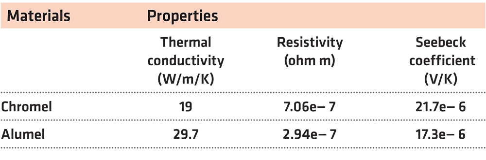
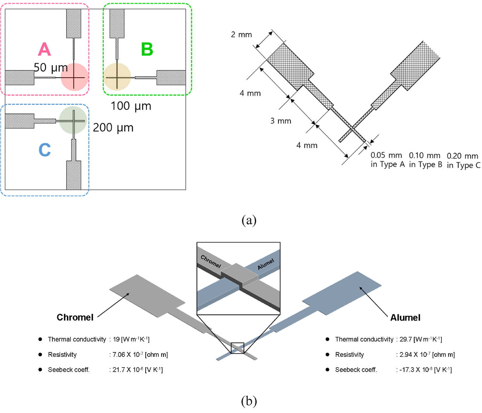
The deposited materials are Chromel and Alumel, which are used in K-type thermocouples, and they were set to (+) and (−) poles, respectively. The initial ambient temperature around the sensor was 25°C. and the other parts in the simulation were set at 50°C. The simulation model calculated the currents while increasing the potential difference between the Chromel (+) and Alumel (−) electrodes from minus-5 to +5 V. The thermal conductivity, resistivity, and Seebeck coefficients were referred from the literature [27,28], and the coefficient values are represented in Table 2.
We simulated design types A, B, and C, which have 0.05 mm, 0.1 mm, and 0.2 mm of Chromel-Alumel electrode overlap length, respectively. Figure 1a and b show the circuit design used for the simulation. The electro pad dimensions were a width of 2 mm and a length of 4 mm, and the connection two-step lines were 3 mm and 4 mm, respectively. The circuit design was determined by the interferences of the cutting tool clamp and cutting tool surface. The circuit dimension used in this simulation is the case study parameter in the experiment.
Electro pad thermoelements were meshed using hexa type in ANSYS. The minimum mesh size was set to 0.025 mm, and the total number of nodes and elements in the geometry were 104706 and 67787, respectively. The contact element was surface-to-surface contact at the interfaces of the electro pad. Thermal contact behavior is a closed contact type; thermal conduction transfers between two contacting surfaces. The conductive heat-transfer equation is defined by Equation 1 [29]:
 where q is the heat flux per area, TCC is the thermal contact conductance coefficient, and Tt and Tc are the temperatures of the contact points at target and contact surfaces, respectively.
The electric contact property is implemented with thermal-electric elements, and the solid coupled field element modeled the electric current conduction. The interface definition is determined by equation (2) [29]:
 where J is the current density for the electric potential degree of freedom (or the electric charge density), ECC is the electric contact conductance for the electric potential degree of freedom (or the electric contact capacitance per unit area), and Vt and Vc are the voltages at the contact points on the target and contact surfaces, respectively.
2.2 Fabrication and performance measurement methods for a thin-film thermocouple (TFTC)
The thermal evaporation method was used to fabricate the K-type TFTC, which included deposition of three materials: Alumel, Chromel, and an insulator. Figure S1 shows the mask used in the experiment. The hot and cold junction in the circuit makes orthogonal contact with the Chromel and Alumel. Four types of junctions, referred to as A, B, C, and D types, were used in this study. A, B, and C junction types have contact areas of 50 µm × 50 µm, 100 µm × 100 µm, and 200 µm × 200 µm, respectively. The electro pad has a width of 2 mm, and this dimension is sufficient to connect the electrode for the DAQ system.
The junction is thin and delicate, which can lead to cracks during deposition. Therefore, we inserted a linked line in the middle of the junction and electrode. Often, a junction crack will be generated during the thermal evaporation process due to the thin linked line. Therefore, first confirmed the influence of the linked line dimension. The D-type junction has an electrode and junction without a step connection line and a square with dimensions of 9 mm × 9 mm to cover the contact and electrode junction. The insulator mask was designed in a 9 mm × 9 mm square shape to cover all junctions.
The thermal deposition method melts the materials using a high current applied to the boat. The initial vacuum pressure was 4.4e−6 Torr. First, we tried to deposit the Alumel material on the flat glass surfaces. The current was ∼130-142 A and the deposition rate was ∼0.03-0.04 nm/s. The boat had a tungsten carbide thickness of 0.5 mm. If the current was set at 100 A, the boat temperature began to increase. Therefore, we set the current to 130 A, and the process was steady with a deposition rate of 0.03 nm/s. The Chromel material was deposited with a deposition rate of ∼0.03-0.05 nm/s with a current of ∼134-155 A. The four types of junctions had a deposited Alumel and Chromel thickness of 100 nm, which was measured using an atomic force microscope.
The TFTC will be to measure the temperature at the cutting interface of the tool-chip. Resistivity measurements and scratch tests were carried out to confirm the TFTC performance. Current-voltage (I-V) tests were used to determine the resistivity of the TFTCs, which presented circuit characteristics. The I-V testing process is described as follows: The deposited sample with the four types of TFTC was held on a hot plate. Then, the I-V test cathode and anode (Keithley 2400 in Figure S2b) were connected to the Alumel and Chromel electro pads. The input voltage was swept from minus-5 to +5 V, and the current values were measured while the hot plate temperature was increased from 50°C to 150°C. The connection wires are used in K-type Extension (OMEGA Engineering, Model: EXPP-K-24S-100).
A scratch test was performed after each material was deposited in a 2.5 mm × 1.5 mm area (thickness of 100 nm) on flat glass substrates. The sample was scratched with a probe with strength increasing gradually, from 0 to 14 mN (NST3 nano scratch tester in Figure S2c).
3. Results and discussion
3.1 FEM simulation comparison with experimental data
Figure 2 shows the simulated data and experimental data for response currents of A-, B-, and C-type junctions. The experimentally fabricated circuit has a thickness of about 75 nm. However, this circuit is very thin relative to the area. Creating a simulation model at a real scale requires making many meshes to improve the mesh quality. This causes an increase in computational time and requires high computational resources. Reducing the amount of mesh saves computational time but reduces mesh quality. The quality of the mesh plays a significant role in the accuracy and stability of numerical computation. Saving computational time while increasing the mesh quality, we used an arbitrary TFTC thickness of approximately 50 µm.
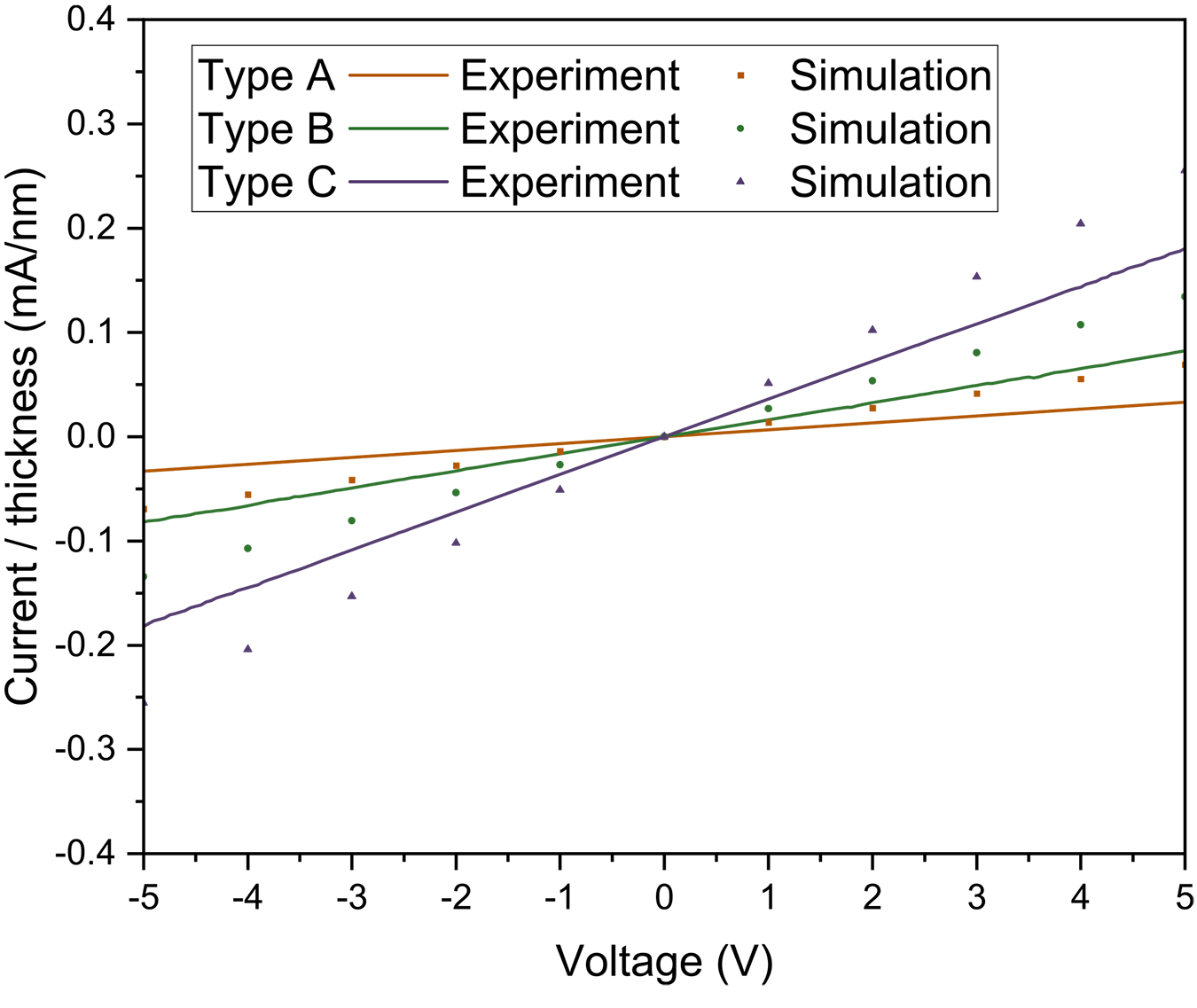
The plot comparing experimental and simulated results in Figure 2 is represented with units of current per thickness (mA/nm). The slope of the current per thickness changes; it increases by junction type in the order of A, B, and C types. The C-type has the largest contact area between the Chromel and Alumel electrodes. The reciprocal of the slope provides the resistance value, and resistance and resistivity are proportional; large resistance means large resistivity [30]. This means that the C-type, which has the largest area, has the smallest resistivity. When the contact area is small, the resistance increases because the area in which electrons can move is limited when a thermo-electromotive force is generated by the thermocouple.
In addition, we can determine the thermoelectric characteristics of the thin-film through the measured resistance [31]. Since the performance may be degraded if the resistance of the contact area is high, the smaller the area, the larger the resistance and possible decrease in thermocouple performance [32]. These results indicate that a large electrode contact area has high sensitivity with respect to the TFTC and the highest performance may be expected in type C.
The simulation model calculated the current density (A/mm2) on the electrode gap area. The current density values of TFTC A, B, and C types were, on average, 9.4e7 A/mm2, 3.1e8 A/mm2, and 3.3e8 A/mm2, respectively (Figure S3). The A-type TFTC has the lowest value of current density, which means its relative resistance is higher than the other TFTC types. The A-type TFTC may exhibit low performance compared to the other types. The B- and C-type TFTCs have current density values of more than 3.0e8 A/mm2; the relative resistance is lower than the A-type TFTC. Therefore, this simulation model is a useable model to approximate TFTC performance according to circuit design.
3.2 Principal TFTC analysis
3.2.1 Influence of the chromel Ni to Cr ratio
The TFTC should exhibit stable performance at high temperatures, such as those in the machining process. Even with exposure to extreme cutting temperatures, a single electrode will typically exhibit low sensitivity depending on increasing temperature. This section discusses the resistivity as a function of ratio of nickel (Ni) to chrome (Cr) in the Chromel used for TFTC fabrication.
The two types of raw Chromel materials available in the commercial market have Ni and Cr ratios of 9:1 and 8:2, which consist of Ni-Cr of 90%-10% and Ni-Cr of 80%-20%, respectively. Alumel has consist of Ni-Al-Mn of 95%-2%-2%, respectively. These two types of Chromel were deposited to experimentally determine the influence of the Ni:Cr ratio. Alumel is only available in a single ratio in the market and is therefore excluded from this section. TFTCs composed of Alumel and Chromel with two ratio types were fabricated using a metal mask with a large area of 1.5 mm × 1.5 mm. Figure S4 shows the measurement setup used to observe the I-V performance as a function of Chromel ratio (8:2 and 9:1) with increasing temperature (by heating the hot plate).
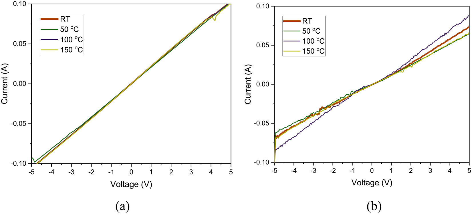
Figure 3 shows the I-V graph according to temperature as Chromel ratios of 8:2 and 9:1, presented in Figure 3a and b, respectively. The resistivity of each sample was calculated to compare their electrical properties. The resistivity (ρ) of a thin-film is defined by Equation 3:
 where, ρ is a resistivity (ohm-cm), t is the TFTC thickness, and I and V are the current and voltage, respectively.
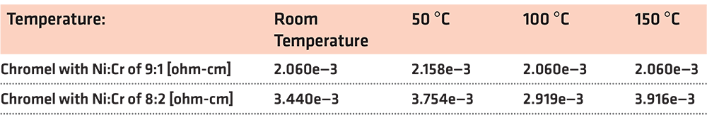
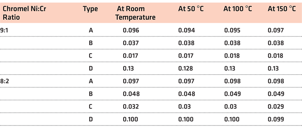
Table 3 presents the TFTC resistivity calculated using Equation 3. Chromel with a Ni:Cr ratio of 9:1 exhibits minimal sensitivity dependence on temperature, while that at a 8:2 ratio shows a slight change. However, the resistivity variation with increasing temperature is low enough to be ignored. Therefore, the TFTC can be composed of Chromel with Ni:Cr ratios of either 9:1 or 8:2. (Cross Alumel).
3.2.2 Influence of TFTC design type
In this section, the influence of the TFTC design type was analyzed to determine their performance. The TFTC types (A, B, C, and D) were presented in Section 3. Chromel (9:1 Ni:Cr ratio) and Alumel were deposited by the thermal deposition process. The detailed process conditions are described in Section 3.
Figure 4 and Figure S5 show an I-V graph of Alumel and Chromel deposited for A, B, C, and D types (Specified measured data shown in Figure 4 (a to d), respectively). Figure 4 represent the I-V slope results for each TFTC type. The resistivity of each TFTC type shows slight differences. These results suggest the I-V behavior and temperature have no relationship in the same contact area. However, the slope of each TFTC type with the same temperature value exhibits significant differences among the TFTC types (Figure S5). The slope of the graph increases as the junction area is increased, suggesting the resistivity of the TFTC decreases as the junction area increases. In addition, types A and D have calculated resistivity values that are almost the same. This means the linked line has little effect on the electrical characteristics of TFTC and is reasonable to design a three-stage structure for a TFTC that will be applied to an actual tool. Figure 5 and Figure S6 show I-V graphs of TFTCs with Alumel and 8:2 Chromel that also confirmed the resistivity in the same area was almost the same with varying temperature. When comparing the TFTC area at the same temperature, the resistivity decreased as the area increased. These results indicate the TFTC Chromel Ni:Cr ratio has minimal influence on performance.
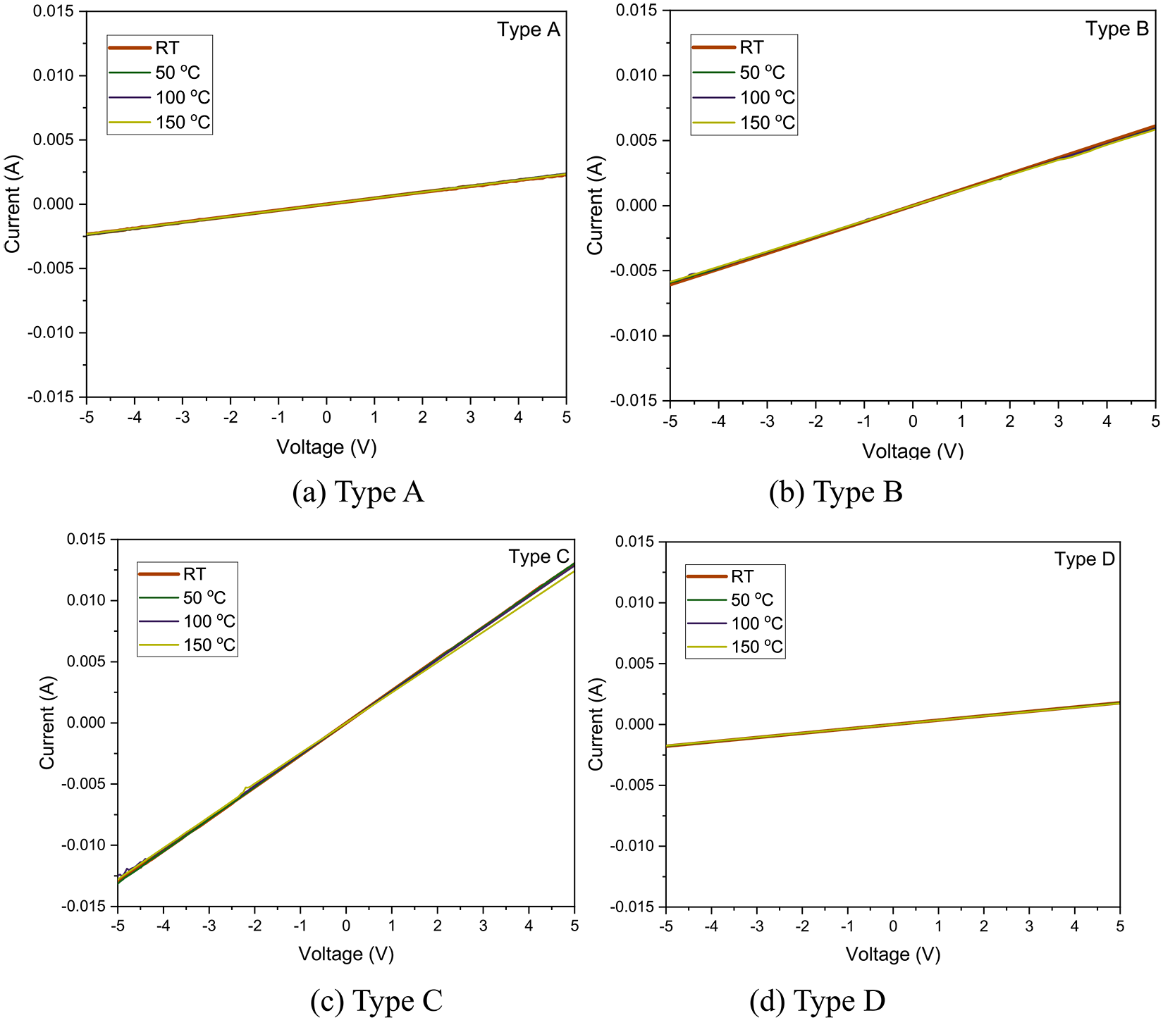
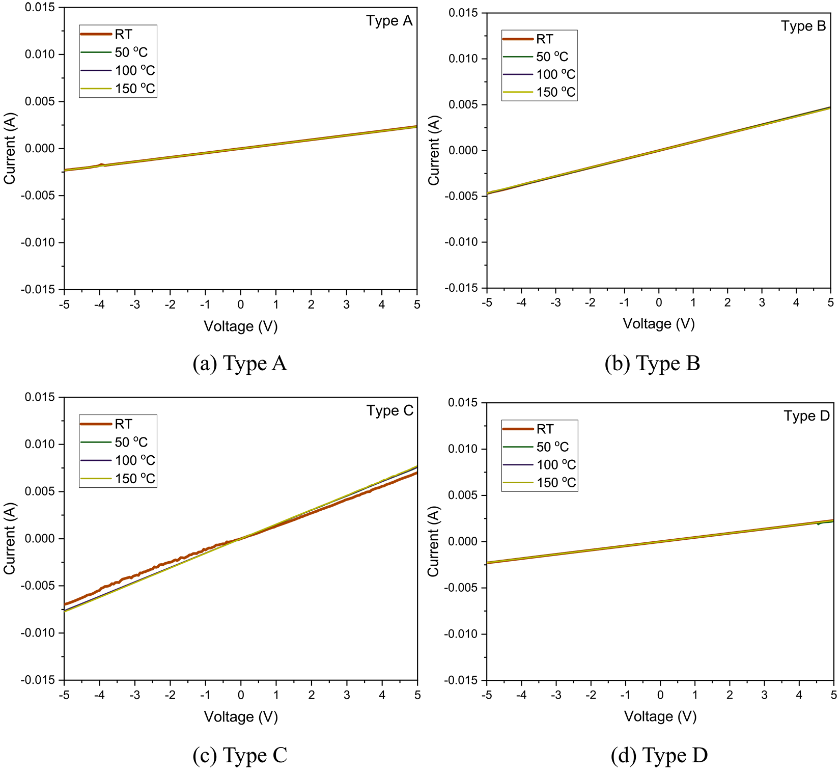
Table 4 shows the calculated resistivity results for each TFTC type. The highest resistivity of 0.13 Ω-cm was observed in the D-type TFTC. This high resistivity means the flowing current is interrupted and leads to reduced performance. Similar results are observed for the D-type TFTC with Chromel Ni:Cr ratio of 8:2. The lowest calculated resistivity values are ∼0.017-0.018 and ∼0.03-0.032 Ω-cm, which correspond to C-type TFTCs with Chromel Ni:Cr ratios of 9:1 and 8:2, respectively. This measurement data means that thermo-electromotive force easily is generated in the C-type design. In section 3.1, C-type design is simulated to have low current density, that means the thermoelectron is a relative easy flow than other designs. No significant change in resistivity is observed with changing temperature. Therefore, the C-type TFTC may be suitable for measuring temperature data during the machining process.
3.2.3 Scratch test results for TFTC adhesion
For the deposited Alumel and Chromel to function properly as sensors, it is important they are well attached to the deposited glass or tool. Therefore, a scratch test was conducted on a sample deposited on a flat glass substrate to determine how much force the materials could withstand. Figure S7 shows an image of the damaged film and the penetration depth. Figure S7- shows the thin Alumel film peeled off at the 0.24-mm point when the applied force was about 6.7 mN. On the other hand, the Chromel thin-film was not wholly peeled off for both Chromel Ni:Cr ratios of 9:1 and 8:2 (Figure S7). However, when looking at the measured image, dig was confirmed to some extent. In addition, when comparing the penetration depth of the two materials, Chromel with a Ni:Cr ratio of 9:1 had a penetration depth of ∼300.3 nm while that with 8:2 ratio was ∼289.3 nm. It was confirmed the degree of peel off was similar for the two Ni:Cr ratios. Therefore, the Chromel adhesion is better than that of Alumel for glass substrates, and there is little difference in adhesion depending on the Ni:Cr ratio of the Chromel.
3.2.4 The EDS component analysis
Figure S8 shows the SEM images (NOVA NanoSEM 230, FEI, USA) for the surfaces of deposited Chromel/Alumel and their analysis compositions by EDS. The SEM images of the Alumel-Chromel film layer are cleared without defects. The EDS data shows that Alumel consists of a weight percent of 77.3% of Ni, 16.2% of Mn, 2% of Al, and 4% of Si. The standard Alumel compositions are 95% of Ni, 2% of Al, 2% of Mn, and 1% of Si. In Chromel, the compositions of it are 75.3% of Ni and 24.7% of Cr. Chromel is also different from standard composition Chromel (9:1, Ni-Cr). The compositions differ from the standard due to the glass substrate, an insulation material, but both deposited films are useful for measuring the temperature. The acquired temperature is described in the next section.
3.3 TFTC performance in acquiring temperature data through data acquisition (DAQ)
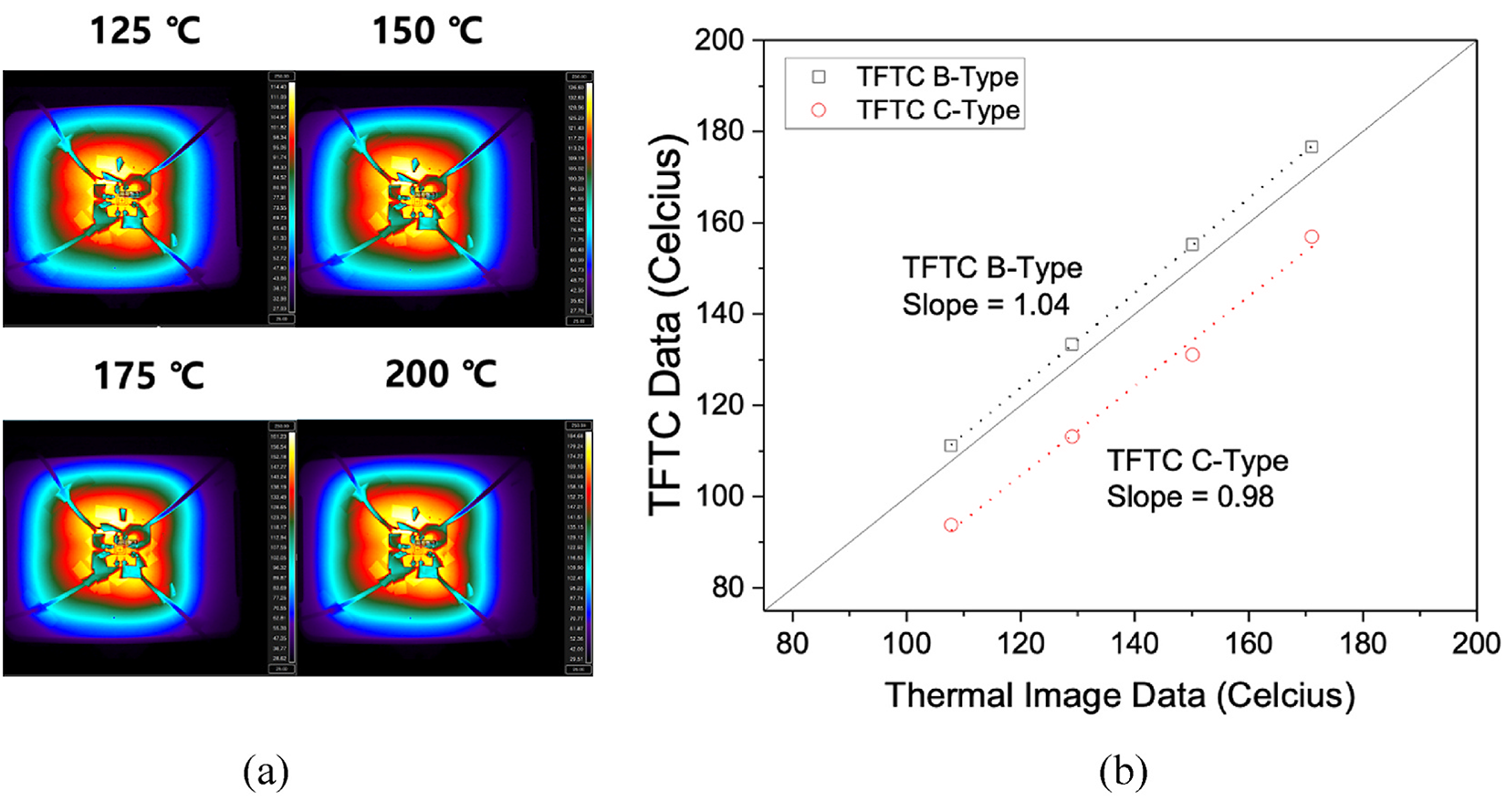
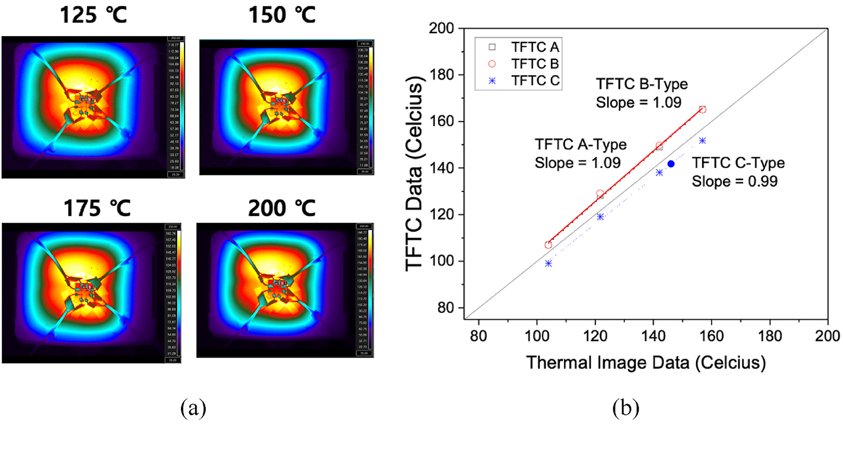
In this section, experiments were conducted to obtain TFTC performance. A DAQ system (WebDAQ 904, measurement computing., Inc) was used to collect the TFTC temperature data while increasing the reference temperature (hot plate temperature). The TFTC data was compared with two types of data collected using an IR-thermal imaging camera (A700sc, FLIR., Inc.) and a K-type thermocouple (Omega Eng.). The IR camera has a 1.5-m minimum focus length, and its measuring range is 67.8 mm in width and 50.8 mm in length. The DAQ system saved the temperature data from the TFTC sensors. The hot plate was used to control the temperature as it heated the back of the TFTC sensors from 125 to 200°C. TFTC sensor data were compared with the IR-imaging data and K-type thermocouple data collected at the same time.
Figure 6 presents the IR-thermal imaging data and a graph comparing the thermal image data to the TFTF sensor data (with an 8:2 Ni:Cr ratio Chromel electrode). The thermal image data is the average of the red rectangular box indicated in the thermal image. Data could not be obtained for the A and D-type TFTCs using the DAQ system. This result is analogous to the trend observed in Table 4 and is due to the small contact area between the (+) and (−) electrode leading to increased resistivity of the TFTC sensor. Slopes of 1.04 and 0.98 were obtained for TFTC B and C types, respectively. Both B and C-type TFTCs have slopes close to a value of one, and their sensitivity is capable of obtaining useable temperature data.
When using Chromel with a Ni:Cr ratio of 9:1 as the TFTC sensor electrode, the DAQ system is able to get data from the A-type TFTC (Figure 7). This Chromel (9:1 Ni:Cr ratio) has low resistivity, as described in the previous section (Figure 3 and Table 3), and the electron flow moves more easily by the electromotive forces. The B and C-type TFTCs have higher sensitivity with this Ni:Cr Chromel ratio. This result is related to the low resistivity of the Chromel with a 9:1 Ni:Cr ratio. Therefore, it is necessary to use the 9:1 Ni:Cr ratio Chromel to obtain electrodes with relatively low resistance and high sensitivity. The high composition of nickel increases the electric forces, improves the performances of the TFTC sensor. The type-B TFTC will be applied to a cutting tool surface for measuring cutting temperatures.
4 Summary and conclusions
The TFTC sensor technique can detect temperatures in a unique environment in many cases, as determined by the literature review, and has potential for measuring cutting temperature. Cutting temperature generation in machining is a significant factor for machining process optimization. This article optimized the TFTC fabrication process for use in the machining field. A simulation model was constructed, using a thermoelectric simulation module in ANSYS to predict the current in different TFTC types. As a result of the simulation, the value of the current responded to increased input voltage similar to that observed in the experiment. This model can be used to predict TFTC sensor performance. TFTC sensor performance was tested for a fundamental TFTC shape with different Chromel raw material ratios (8:2 and 9:1 of nickel and chrome). The TFTC sensor with Chromel, having an 8:2 Ni:Cr ratio, exhibited unstable sensitivity with increasing temperature, while the TFTC sensor with Chromel, having a 9:1 Ni:Cr ratio, exhibited stable sensitivity. A comparison of different TFTC types was made to evaluate their performance. If the electrode contact area of the TFTC sensor is small, its sensitivity was low. The C-type TFTC had the largest electrode contact area and the highest sensitivity. However, no sensitivity variation was observed in the TFTC sensor with increasing temperature. TFTC sensor resistivity was calculated using I-V data; the C-type TFTC had the lowest resistivity due to its largest electrode contact area. When Chromel with a Ni:Cr ratio of 9:1 was used, the resistivity was lower than that with a Ni:Cr ratio of 8:2. The Alumel electrode exhibited lower scratch strength compared to the Chromel electrode, and the Chromel Ni:Cr ratio had no influence on scratch strength. The temperature data was obtained using a DAQ system connected to the TFTC sensors. The B- and C-type TFTCs with an 8:2 Ni:Cr ratio Chromel electrode could sense temperature variation while the other TFTC sensors did not operate under the same conditions. A-, B-, and C-type TFTCs with a 9:1 Ni:Cr ratio Chromel electrode were able to detect the temperature data with the DAQ system. The highest sensitivity was observed for the B-type TFTC with a 9:1 Ni:Cr ratio Chromel electrode.
In conclusion, a TFTC sensor for a DAQ system used during machining operation should be constructed with a large electrode contact area and a Chromel Ni:Cr ratio of 9:1 for high performance. The TFTC sensor with optimized design and fabrication process determined by this study will be integrated on tool rake surfaces similar to those illustrated in Figure S9. This sensor technology will be able to measure the cutting temperature during machining using unique materials (e.g., Inconel, titanium, carbon-fiber reinforced polymer, or biomaterials, such as bone), and will be a useful technology to analyze their cutting principles.
Credit authorship contribution statement
Dong Min Kim: Writing – original draft, Formal analysis, Conceptualization. Hee Jung Kwak: Writing – original draft, Data curation. Dong Yeol Shin: Writing – original draft, Software, Data curation. Jin Ho Park: Data curation. Jun Young Kim: Writing – review & editing, Writing – original draft, Resources, Formal analysis, Conceptualization.
Declaration of competing interest
The authors declare that they have no known competing financial interests or personal relationships that could have appeared to influence the work reported in this paper.
Appendix A: Supplementary data
Supplementary data to this article can be found online at https://doi.org/10.1016/j.heliyon.2024.e26128.
Acknowledgments
This research was supported by the National Research Foundation of Korea (NRF) funded by the Ministry of Science and ICT of Korea (2020R1C1C1008113). Also, this work was supported by the National Research Foundation of Korea (NRF) grant funded by the Korea government (MSIT) (No. RS-2023-00222166). This research was also supported by the GNU-Samsung Display Center.
References
- E. Usui, T. Shirakashi, T. Kitagawa. Analytical prediction of cutting tool wear. Wear, 100 1–3 (1984), pp. 129-151.
- M. Tiffe, R. Aßmuth, J. Saelzer, D. Biermann. Investigation on cutting edge preparation and FEM assisted optimization of the cutting edge micro shape for machining of nickel-base alloy. Prod. Eng. Res. Dev., 13 (2019), pp. 459-467.
- T.H.C. Childs, P.J. Arrazola, P. Aristimuno, A. Garay, IrantzuSacristan. Ti6Al4V metal cutting chip formation experiments and modelling over a wide range of cutting speeds. J. Mater. Process. Technol., 255 (2018), pp. 898-913.
- S. Imbrogno, S. Rinaldi, D. Umbrello, L. Filice, R. Franchi, A.D. Prete. A physically based constitutive model for predicting the surface integrity in machining of Waspaloy Mater. Des., 152 15 (2018), pp. 140-155.
- A. Bagherzadeh, E. Budak. Investigation of machinability in turning of difficult-to-cut materials using a new cryogenic cooling approach. Tribol. Int., 119 (2018), pp. 510-520.
- D. Soler, P.X. Aristimuño, M. Saez-de-Buruaga, A. Garay, P.J. Arrazola. New calibration method to measure rake face temperature of the tool during dry orthogonal cutting using thermography. Appl. Therm. Eng., 137 5 (2018), pp. 74-82.
- J. Saelzer, S. Berger, I. Iovkov, A. Zabel, D. Biermann. In-situ measurement of rake face temperatures in orthogonal cutting. CIRP Ann-Manuf. Technol., 69 (2020), pp. 61-64.
- X. Zhao, K. Yang, Y. Wang, Y. Chen, H. Jiang. Stability and thermoelectric properties of ITON:Pt thin film thermocouples. J. Mater. Sci. Mater. Electron., 27 (2016), pp. 1725-1729.
- X. Zhao, H. Li, Y. Chen, H. Jiang. Preparation and thermoelectric characteristics of ITO/Pt thin film thermocouples on Ni-based superalloy substrate. Vacuum, 140 (2017), pp. 116-120.
- A. Basti, T. Obikawa, J. Shinozuka. Tools with built-in thin film thermocouple sensors for monitoring cutting temperature. Int. J. Mach. Tools Manuf., 47 5 (2007), pp. 793-798.
- J. Shinozuka, A. Basti, T. Obikawa. Development of cutting tool with built-in thin film thermocouples for measuring high temperature fields in metal cutting processes. J. Manuf. Sci. Eng.-Trans. ASME., 130 3 (2008), Article 034501.
- D. Werschmoeller, K. l Ehmann, X. Li. Tool embedded thin film microsensors for monitoring thermal phenomena at tool-workpiece interface during machining. J. Manuf. Sci. Eng.-Trans. ASME., 133 2 (2011), Article 021007.
- D. Werschmoeller, X. Li. Measurement of tool internal temperatures in the tool–chip contact region by embedded micro thin film thermocouples. J. Manuf. Process., 13 2 (2011), pp. 147-152.
- D. Werschmoeller, X. Li, K. Ehmann. Measurement of transient tool-internal temperature fields during hard turning by insert-embedded thin film sensors. J. Manuf. Sci. Eng.-Trans. ASME, 134 6 (2012), Article 061004.
- L. Li, B. Li, K.F. Ehmann, X. Li. A thermo-mechanical model of dry orthogonal cutting and its experimental validation through embedded micro-scale thin film thermocouple arrays in PCBN tooling. Int. J. Mach. Tools Manuf., 70 (2013), pp. 70-87.
- T. Li, T. Shi, Z. Tang, G. Liao, J. Duan, J. Han, Z. He. Real-time tool wear monitoring using thin-film thermocouple. J. Mater. Process. Technol., 288 (2021), Article 116901.
- Z. He, T. Shi, J. Xuan, T. Li. Research on tool wear prediction based on temperature signals and deep learning. Wear, 478–479 (2021), Article 203902.
- S. Kesriklioglu, J.D. Morrow, F.E. Pfefferkorn. Tool–chip interface temperature measurement in interrupted and continuous oblique cutting. J. Manuf. Sci. Eng.-Trans. ASME, 140 5 (2018), Article 51013.
- J. Li, B. Tao, S. Huang, Z. Yin. Built-in thin film thermocouples in surface textures of cemented carbide tools for cutting temperature measurement. Sens. Actuator A-Phys., 279 15 (2018), pp. 663-670.
- J. Li, B. Tao, S. Huang, Z. Yin. Cutting tools embedded with thin film thermocouples vertically to the rake face for temperature measurement. Sens. Actuator A-Phys., 296 (1) (2019), pp. 392-399.
- T. Li, T. Shi, Z. Tang, G. Liao, J. Han, J. Duan. Temperature monitoring of the tool-chip interface for PCBN tools using built-in thin-film thermocouples in turning of titanium alloy. J. Mater. Process. Technol., 275 (2020), Article 116376.
- T.A. Yemata, Y. Zheng, A.K.K. Kyaw, X. Wang, J. Song, W.S. Chin, J. Xu. Modulation of the doping level of PEDOT: PSS film by treatment with hydrazine to improve the Seebeck coefficient. RSC Adv., 10 (3) (2020), pp. 1786-1792.
- Nitin Saxena, et al. Ionic liquids as post-treatment agents for simultaneous improvement of Seebeck coefficient and electrical conductivity in PEDOT: PSS Films ACS Appl. Mater. Interfaces, 11 (8) (2019), pp. 8060-8071.
- Z. Huang, D. Wang, C. Li, J. Wang, G. Wang, L.D. Zhao. Improving the thermoelectric performance of p-type PbSe via synergistically enhancing the Seebeck coefficient and reducing electronic thermal conductivity. J. Mater. Chem. A, 8 (9) (2020), pp. 4931-4937.
- A. Gunawan, P. Tarakeshwar, V. Mujica, D.A. Buttry, P.E. Phelan. “Improving Seebeck coefficient of thermoelectrochemical cells by controlling ligand complexation at metal redox centers. Appl. Phys. Lett., 118 (2021), p. 25.
- Xin Guan, Jianyong Ouyang. Enhancement of the Seebeck coefficient of organic thermoelectric materials via energy filtering of charge carriers. CCS Chem., 3 (10) (2021), pp. 2415-2427.
- Concept Alloys Intellectual Property, Concept Alloys (2016).
- E. Rathakrishnan. Instrumentation, Measurements and Experiments in Fluids. CRC Press (2007).
- ANSYS Contact Technology Guide, Ansys (2004).
- M. Naftaly, S. Das, J. Gallop, K. Pan, F. Alkhalil, D. Kariyapperuma, S. Constant, C. Ramsdale L. Hao. Sheet resistance measurements of conductive thin films: a comparison of techniques. Electronics, 10 8 (2021), p. 960.
- K.G. Kreider, G. Gillen. High temperature materials for thin-film thermocouples on silicon wafers. Thin Solid Films, 376 (1) (2000), pp. 32-37.
- F.I. Igorevich. Thermocouple Condition Monitoring Using Thermocouple Resistance. Experimental Study IEEE (2020), Article 19691094.
© 2024 The Authors. Published by Elsevier Ltd. This is an open access article (https://www.sciencedirect.com/science/article/pii/S2405844024021595) under the CC BY-NC-ND license (http://creativecommons.org/licenses/by-nc-nd/4.0/). This article has been edited to conform to the style of Thermal Processing magazine.


 general practice for CQI-9 and AMS2750E")


